- 您现在的位置:买卖IC网 > Sheet目录474 > MAX7060EVKIT+ (Maxim Integrated)EVAL KIT MAX7060
�� �
�
�MAX7060�
�280MHz� to� 450MHz� Programmable�
�ASK/FSK� Transmitter�
�SDI_PWR1�
�SCLK_PWR0�
�Table� 27.� Output� Power� Settings�
�dB� BELOW�
�P� MAX�
�0� 0� 0�
�0� 1� 3�
�1� 0� 6�
�When� the� frequency� is� set� to� 315MHz,� the� PA� capaci-�
�tance� increases� by� the� programmed� value.�
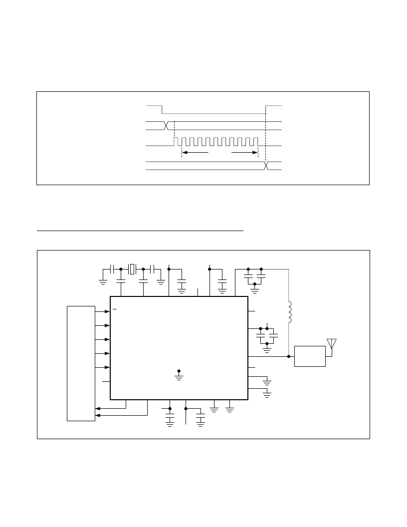
�Figure� 8� illustrates� how� to� set� the� capacitance.� It� begins�
�with� the� ENABLE� pin� pulled� low.� The� frequency� is�
�sampled� at� the� rising� edge� of� the� first� pulse.� Pulses�
�2–11� set� the� capacitance� code� to� 0x0A� (10dec),� which�
�is� approximately� 2.5pF.� The� ENABLE� pin� is� then� pulled�
�1�
�1�
�10�
�high� to� finish� the� setting.�
�Frequency� Deviation�
�Reset� pin� 19� (� CS� _DEV)� to� 0� for� 32kHz� (� Q� 16kHz)� FSK�
�deviation� and� 1� for� 100kHz� (� Q� 50kHz)� FSK� deviation.�
�Transmitter� Power�
�Set� SDI_PWR1� (pin� 20)� and� SCLK_PWR0� (pin� 21)� to� four�
�power� settings� (relative� to� the� maximum� power� setting).�
�Note� that� at� battery� voltages� below� 3V,� the� top� two� power�
�settings� are� compressed� and� the� power� difference� is�
�less� than� 3dB.�
�PA� Variable� Capacitor� Setting�
�In� manual� mode,� capacitance� can� be� added� to� the� PA�
�output� for� one� selected� frequency.� This� allows� the� user�
�to� adjust� the� matching� network� when� switching� between�
�two� frequencies� in� the� manual� selection� table,� or� for�
�switching� to� one� frequency� that� is� significantly� different�
�from� the� others� in� the� table.� The� user� can� set� the� capaci-�
�tance� by� resetting� the� ENABLE� pin� to� a� logic-low,� then�
�selecting� the� frequency� for� which� the� variable� capacitor�
�is� to� be� added� from� the� seven� possible� settings,� and�
�then� sending� a� stream� of� 1� to� 32� pulses� through� the� DIN�
�pin.� The� first� pulse� is� used� to� reset� the� internal� capacitor�
�counter� and� to� latch� the� selected� frequency.� After� the� first�
�pulse,� the� remaining� number� of� pulses� sent� equals� the�
�variable� capacitor� setting.� When� the� ENABLE� pin� goes�
�high,� the� capacitor� setting� for� the� specified� frequency� is�
�set,� so� that� it� adds� the� programmed� capacitance� to� the�
�PA� when� the� chosen� frequency� is� selected.� This� scheme�
�must� be� executed� only� once� to� set� the� value� of� the� vari-�
�able� capacitor.�
�For� example,� a� user� can� operate� the� MAX7060� at�
�315MHz� and� 433.92MHz� into� a� narrowband� antenna�
�by� resetting� the� ENABLE� pin� low,� setting� the� FREQ0,�
�FREQ1,� FREQ2� pins� to� 001� (315MHz),� and� sending� the�
�appropriate� number� of� pulses� into� the� DIN� pin,� and� then�
�setting� the� ENABLE� pin� high.� When� the� frequency� is� set�
�to� 433.92MHz� (or� any� other� frequency� in� the� table� except�
�315MHz),� no� capacitance� is� added� to� the� PA� output.�
�Maxim� Integrated�
�Emulation� Mode� Settings�
�All� the� settings� available� through� the� manual� mode� of�
�operation� are� also� easily� accessible� in� the� SPI� mode.�
�This� mode� is� called� emulation� mode,� whereby� only� writ-�
�ing� one� or� two� registers,� the� whole� transmitter� can� be�
�configured.� The� Conf2� register� controls� this� mode.�
�The� emulation� mode� is� a� subset� of� SPI� mode.� It� gives� SPI�
�users� the� capability� to� operate� the� part� by� programming�
�just� one� or� two� registers� instead� of� all� registers.�
�Since� it� is� still� SPI� mode,� pins� 5,� 6,� and� 7� (FREQ0,� FREQ1,�
�and� FREQ2)� must� be� pulled� low.� The� Conf2� register� is�
�the� only� register� that� needs� to� be� programmed.� Setting�
�bit� 7� (fixed)� to� 1� enables� this� mode.� Bit� 6� (fxmode)� is�
�equivalent� to� pin� 1� (GPO2_MOD)� in� manual� mode.� Bits�
�5� and� 4� (fxpwr[1:0])� are� equivalent� to� pin� 20� and� 21�
�(SDI_PWR1� and� SCLK_PWR0)� in� manual� mode.� Bit� 3�
�(fxhdev)� is� equivalent� to� pin� 19� (� CS� _DEV)� in� manual�
�mode.� Bits� 2,� 1,� and� 0� (fxfrq[2:0])� are� equivalent� to� pins�
�5,� 6,� and� 7� (FREQ0,� FREQ1,� and� FREQ2)� in� manual�
�mode.�
�Similar� to� manual� mode,� the� PA� capacitor� setting� in� the�
�emulation� mode� can� be� done� by� toggling� the� DIN� pin�
�with� the� ENABLE� pin� low.� In� addition,� the� capacitor� set-�
�ting� can� also� be� done� by� directly� writing� to� the� capacitor�
�register� (bits� 4:0� of� the� Conf1� register,� cap[4:0]).� As� long�
�as� the� capacitor� register� value� is� not� zero,� the� capacitor�
�value� sent� in� by� toggling� the� DIN� pin� is� ignored.�
�Control� Interface� Considerations�
�When� operating� the� MAX7060� with� a� +4.5V� to� +5.5V�
�supply� voltage,� the� CS� _DEV,� SCLK_PWR0,� SDI_PWR1,�
�FREQ0,� FREQ1,� FREQ2,� ENABLE,� DIN,� and� LSHDN�
�pins� can� be� driven� by� a� microcontroller� with� either� 3V� or�
�5V� interface� logic� levels.� When� operating� the� MAX7060�
�with� a� +2.1V� to� +3.6V� supply,� the� microcontroller� must�
�produce� logic� levels� that� conform� to� the� V� IH� and� V� IL�
�specifications� in� the� DC� Electrical� Characteristics� for� the�
�MAX7060.�
�27�
�发布紧急采购,3分钟左右您将得到回复。
相关PDF资料
MAX8506EVKIT
EVAL KIT FOR MAX8506
MAX8582ETB+T
IC CONV 1.5MHZ CDMA 10-TDFN
MAX9635ESA+
IC AMBIENT LIGHT SENSOR 8NSOIC
MAX9930EVKIT+
KIT EVAL FOR MAX9930
MAX9947ETE+
TXRX AISG INTEGRATED 16TQFN
MAX9981ETX+D
IC MIXER DUAL SIGE 36-QFN
MAX9981EVKIT
EVAL KIT FOR MAX9981
MAX9982ETP+D
IC MIXER HI LINEAR SIGE 20-TQFN
相关代理商/技术参数
MAX706AP
制造商:MAXIM 制造商全称:Maxim Integrated Products 功能描述:+3V Voltage Monitoring, Low-Cost uP Supervisory Circuits
MAX706APEPA
制造商:MAXIM 制造商全称:Maxim Integrated Products 功能描述:+3V Voltage Monitoring, Low-Cost uP Supervisory Circuits
MAX706APEPA+
功能描述:监控电路 Single uPower Supervisor RoHS:否 制造商:STMicroelectronics 监测电压数: 监测电压: 欠电压阈值: 过电压阈值: 输出类型:Active Low, Open Drain 人工复位:Resettable 监视器:No Watchdog 电池备用开关:No Backup 上电复位延迟(典型值):10 s 电源电压-最大:5.5 V 最大工作温度:+ 85 C 安装风格:SMD/SMT 封装 / 箱体:UDFN-6 封装:Reel
MAX706APESA
制造商:MAXIM 制造商全称:Maxim Integrated Products 功能描述:+3V Voltage Monitoring, Low-Cost uP Supervisory Circuits
MAX706APESA+
功能描述:监控电路 Single uPower Supervisor RoHS:否 制造商:STMicroelectronics 监测电压数: 监测电压: 欠电压阈值: 过电压阈值: 输出类型:Active Low, Open Drain 人工复位:Resettable 监视器:No Watchdog 电池备用开关:No Backup 上电复位延迟(典型值):10 s 电源电压-最大:5.5 V 最大工作温度:+ 85 C 安装风格:SMD/SMT 封装 / 箱体:UDFN-6 封装:Reel
MAX706APESA+T
功能描述:监控电路 Single uPower Supervisor RoHS:否 制造商:STMicroelectronics 监测电压数: 监测电压: 欠电压阈值: 过电压阈值: 输出类型:Active Low, Open Drain 人工复位:Resettable 监视器:No Watchdog 电池备用开关:No Backup 上电复位延迟(典型值):10 s 电源电压-最大:5.5 V 最大工作温度:+ 85 C 安装风格:SMD/SMT 封装 / 箱体:UDFN-6 封装:Reel
MAX706APEUA
制造商:MAXIM 制造商全称:Maxim Integrated Products 功能描述:+3V Voltage Monitoring, Low-Cost uP Supervisory Circuits
MAX706APEUA+
功能描述:监控电路 Single uPower Supervisor RoHS:否 制造商:STMicroelectronics 监测电压数: 监测电压: 欠电压阈值: 过电压阈值: 输出类型:Active Low, Open Drain 人工复位:Resettable 监视器:No Watchdog 电池备用开关:No Backup 上电复位延迟(典型值):10 s 电源电压-最大:5.5 V 最大工作温度:+ 85 C 安装风格:SMD/SMT 封装 / 箱体:UDFN-6 封装:Reel